
Chapter 12
Fundamentals of Electricity & Electronics
Identification of Transistors
Figure 12-224 illustrates some of the more common transistor lead identifications. The methods of identifying leads vary due to a lack of a standard and require verification using manufacturer information to properly identify. However, a short description of the common methods is discussed below.
Figure 12-224D shows an oval-shaped transistor. The collector lead in this case is identified by the wide space between it and the lead for the base. The final lead at the far left is the emitter. In many cases, colored dots indicate the collector lead, and short leads relative to the other leads indicate the emitter. In a conventional power diode, as seen in Figure 12-224E, the collector lead is usually a part of the mounting bases, while the emitter and collector are leads or tines protruding from the mounting surface.
Field Effect Transistors
Another transistor design that has become more important than the bipolar transistor is the field-effect transistor (FET). The primary difference between the bipolar transistor and the FET is that the bipolar transistor has two PN junctions and One category is called the junction FET (JFET), which has only one PN junction. The other category is known as the enhancement-type or metal-oxide JET (MOSFET).
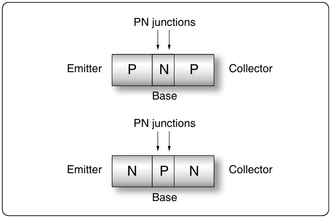
Figure 12-225 shows the basic construction of the JFET and the schematic symbol. In this figure, it can be seen that the drain (D) and source (S) are connected to an N-type material, and the gate (G) is connected to the P-type material. With gate voltage Vgg set to 0 volts and drain voltage Vdd set to some positive voltage, a current flows between the source and the drain, through a narrow band of N-material. If then, Vgg is adjusted to some negative voltage, the PN junction is reverse biased, and a depletion zone (no charge carriers) is established at the PN junction. By reducing the region of noncarriers, it has the effect of reducing the dimensions of the N-channel, resulting in a reduction of source to drain current.
Because JFETs are voltage-controlled devices, they have some advantages over the bipolar transistor. One such advantage is that because the gate is reverse biased, the circuit that it is connected to sees the gate as a very high resistance. This means that the JFET has less of an insertion influence in the circuit. The high resistance also means that less current is used.
Like many other solid-state devices, careless handling and static electricity can damage the JFET. Technicians should take all precautions to prevent such damage.
Metal-Oxide-Semiconductor FET (MOSFET)
Figure 12-226 illustrates the general construction and the schematic symbol of the MOSFET transistor. The biasing arrangement for the MOSFET is essentially the same as that for the JFET. The term “enhancement” comes from the idea that when there is no bias voltage applied to the gate (G), then there is no channel for current conduction between the increases. The schematic symbol reflects this characteristic by using a broken line to indicate that the channel does not exist without a gate bias.
Common Transistor Configurations
A transistor may be connected in one of three different configurations: common-emitter (CE), common-base (CB), and common-collector (CC). The term “common” is used to indicate which element of the transistor is common to both the input and the output. Each configuration has its own characteristics, which makes each configuration suitable for particular applications. A way to determine what configuration you may find in a circuit is to first determine which of the three transistor elements is used for the input signal. Then, determine the element used for the output signal. At that point, the remaining element, (base, emitter, or collector) is the common element to both the input and output, and thus you determine the configuration.
Common-Emitter (CE) Configuration
This is the configuration most commonly used in amplifier output signal is taken off the collector-emitter junction, which is reverse biased (high resistance). Then the emitter is the common element to both input and output circuits. [Figure 12-227]
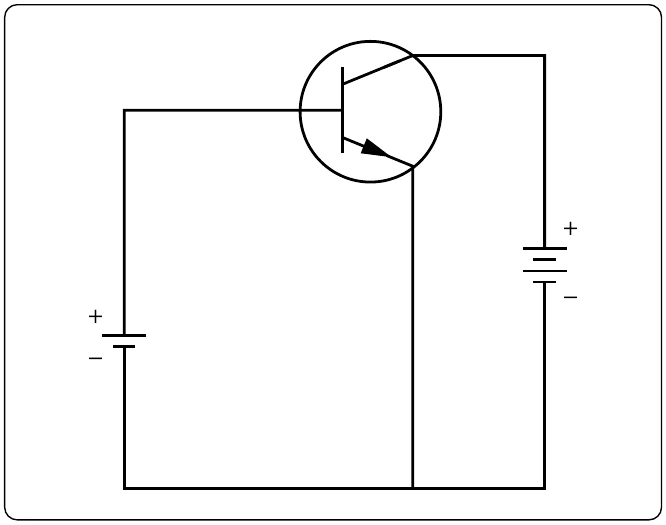
When the transistor is connected in a CE configuration, the input signal is injected between the base and emitter, which is a low-resistance, low-current circuit. As the input signal goes positive, it causes the base to go positive relative to the emitter. This causes a decrease in the forward bias, which in turn reduces the collector current IC and increases the collector voltage (EC being more negative). During the negative portion of the input signal, the voltage on the base is driven more negative relative to the emitter. This increases the forward bias and allows an increase in collector current IC and a decrease in collector voltage (EC being less negative and going positive). The collector current, which flows through the reverse-biased junction, also flows through a high-resistance load resulting in a high level of amplification.
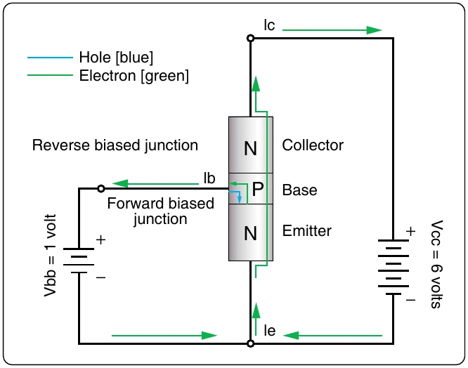
Because the input signal to the CE goes positive when the output goes negative, the two signals are 180° out of phase. This is the only configuration that provides a phase reversal. The CE is the most popular of the three configurations because it has the best combination of current and voltage gain. Gain is a term used to indicate the magnitude of amplification. Each transistor configuration has its unique gain characteristics even though the same transistors are used.