
Chapter 12
Fundamentals of Electricity & Electronics
Power Rectifier Diodes
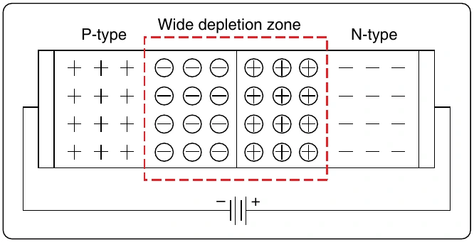
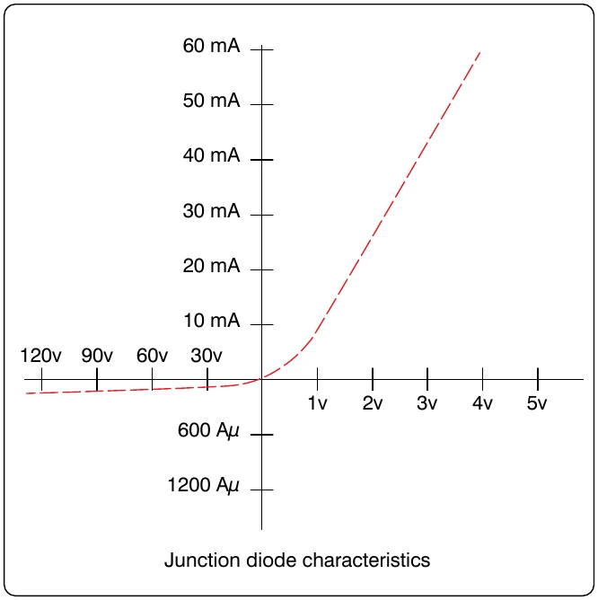
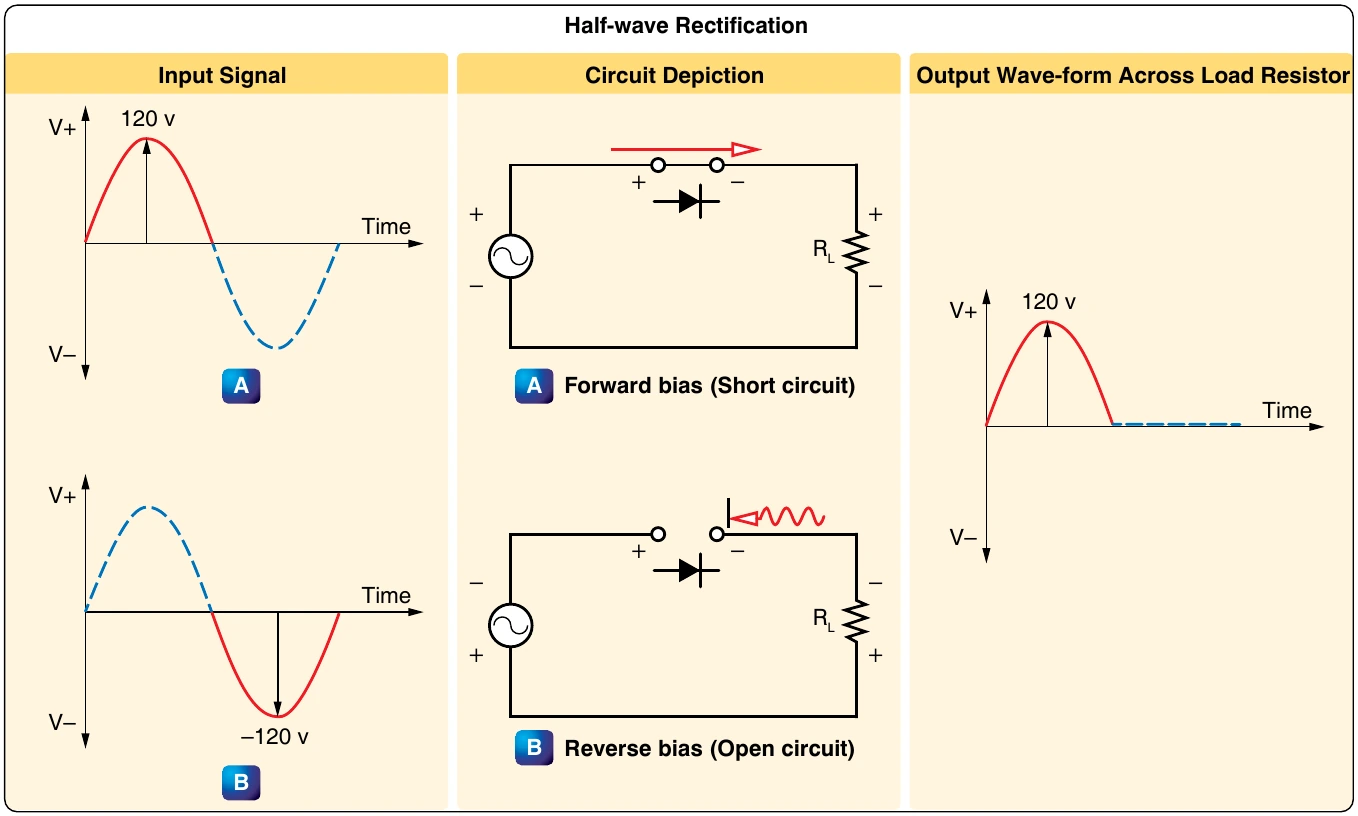
The rectifier diode is usually used in applications that require high current, such as power supplies. The range in which the diode can handle current can vary anywhere from one ampere to hundreds of amperes. One common example of diodes is the series of diodes, part numbers 1N4001 to 1N4007. The “1N” indicates that there is only one PN junction, or that the device is a diode. The average current carrying range for these rectifier diodes is about one ampere with a peak inverse voltage between 50 volts to 1,000 volts. Larger rectifier diodes can carry currents up to 300 amperes when forward biased and have a peak inverse voltage of 600 volts. A recognizable feature of the larger rectifier diodes is that they are encased in metal in order to provide a heat Zener diodes (sometimes called “breakdown diodes”) are designed so that they break down (allow current to pass) when the circuit potential is equal to or in excess of the desired reverse bias voltage. The range of reverse bias breakdown-voltages commonly found can range from 2 volts to 200 volts depending on design. Once a specific reverse bias voltage has been reached, the diode conducts and behaves like a constant voltage source. Within the normal operating range, the zener functions as a voltage regulator, waveform clipper, and other related functions. Below the desired voltage, the zener blocks the circuit like any other diode biased in the reverse direction. Because the zener diode allows free flow in one direction when it is used in an AC circuit, two diodes connected in opposite directions must be used. This takes care of both alternations of current. Power ratings of these devices range from about 250 milliwatts to 50 watts.
Special Purpose Diodes
The unique characteristics of semiconductor material have allowed for the development of many specialized types of diodes. A short description of some of the more common diode types is given for general familiarization. [Figure 12-219]
Light-Emitting Diode (LED)
In a forward biased diode, electrons cross the junction and fall into holes. As the electrons fall into the valence band, they radiate energy. In a rectifier diode, this energy is dissipated as heat. However, in the light-emitting diode (LED), the energy is dissipated as light. By using elements such as gallium, arsenic, and phosphorous, an LED can be designed to radiate colors, such as red, green, yellow, blue, and infrared light. LEDs that are designed for the visible light portion of the spectrum are useful for instruments, indicators, and even cabin lighting. The advantages of the LED over the incandescent lamps are longer life, lower voltage, faster on and off operations, and less heat.
The liquid crystal display (LCD) has an advantage over the LED in that it requires less power to operate. Where LEDs commonly operate in the milliwatt range, the LCD operates in the microwatt range. The liquid crystal is encapsulated between two glass plates. When voltage is not applied to the LCD, the display is clear. However, when a voltage is applied, the result is a change in the orientation of the atoms of the crystals. The incident light is then reflected in a different direction. A frosted appearance results in the regions that have voltage applied and permits distinguishing of numeric values.
Photodiode
Thermal energy produces minority carriers in a diode. The higher the temperature, the greater the current in a reverse current diode. Light energy can also produce minority carriers. By using a small window to expose the PN junction, a photodiode can be built. When light falls upon the junction of a reverse-biased photodiode, electrons-hole pairs are created inside the depletion layer. The stronger the light, the greater the number of light-produced carriers, which in turn causes a greater magnitude of reverse-current. Because of this characteristic, the photodiode can be used in light detecting circuits.
Varactors
The varactor is simply a variable-capacitance diode. The reverse voltage applied controls the variable-capacitance of the diode. The transitional capacitance decreases as the reverse voltage is increasingly applied. In many applications, the varactor has replaced the old mechanically tuned capacitors. Varactors can be placed in parallel with an inductor and provide a resonant tank circuit for a tuning circuit. By simply varying the reverse voltage across the varactor, the resonant frequency of the circuit can be adjusted.
Schottky Diodes
Schottky diodes are designed to have metal, such as gold, silver, or platinum, on one side of the junction and doped silicon, usually an N-type, on the other side of the junction. This type of a diode is considered a unipolar device because free electrons are the majority carrier on both sides of the junction. The Schottky diode has no depletion zone or charge storage, which means that the switching time can be as high as 300 MHz. This characteristic exceeds that of the bipolar diode.
Diode Identification
Figure 12-218 illustrates a number of methods employed for identifying diodes. Typically manufacturers place some form of an identifier on the diode to indicate which end is the anode and which end is the cathode. Dots, bands, colored bands, the letter ‘k’ or unusual shapes indicate the cathode end of the diode.
Introduction to Transistors
The transistor is a three-terminal device primarily used to amplify signals and control current within a circuit. [Figure 12-220] The basic two-junction semiconductor must have one type of region sandwiched between two of the other type. The three regions in a transistor are the collector (C), which is moderately doped, the emitter (E), which is heavily doped, and the base (B), which is significantly less doped. The alternating layers of semiconductor material type provide the common commercial name for each type of transistor. The interface between the layers is called a junction. Selenium and germanium diodes previously discussed are examples of junction diodes. Note that the sandwiched layer or base is significantly thinner than the collector or the emitter. In general, this permits a “punching through” action for the carriers passing between the collector and emitter terminals.