
Chapter 12
Fundamentals of Electricity & Electronics
Each time an electron crosses the PN junction, it creates a pair of ions. Figure 12-211 shows this area outlined by dashed lines. The circled plus signs and the circled negative signs are the positive and negative ions, respectively. These ions are fixed in the crystal and do not move around like electrons or holes in the conduction band. Thus, the depletion zone constitutes a layer of a fixed charge. An electrostatic field, represented by a small battery in Figure 12-211, is established across the junction between the oppositely charged ions.
The junction barrier is an electrostatic field, which has been created by the joining of a section of N-type and P-type material. Because holes and electrons must overcome this field to cross the junction, the electrostatic field is usually called a barrier. Because there is a lack or depletion of free electrons and holes in the area around the barrier, this area is called the depletion region. [Figure 12-211] As the diffusion of electrons and holes across the junction continue, the strength of the electrostatic field increases until it is strong enough to prevent electrons or holes from crossing over. At this point, a state of equilibrium exists, and there is no further movement across the junction. The electrostatic field created at the junction by the ions in the depletion zone is called a barrier.
Forward Biased Diode
Figure 12-212 illustrates a forward biased PN junction. When an external voltage is applied to a PN junction, it is called bias. In a forward biased PN junction or diode, the negative voltage source is connected to the N-type material and the positive voltage source is connected to the P-type material. In this configuration, the current can easily flow. If a battery is used to bias the PN junction and it is connected in such a way that the applied voltage opposes the junction field, it has the effect of reducing the junction barrier and consequently aids in the current flow through the junction.
The electrons move toward the junction and the right end of the diode becomes slightly positive. This occurs because electrons at the right end of the diode move toward the junction and leave positively charged atoms behind. The positively charged atoms then pull electrons into the diode from the negative terminal of the battery.
When electrons on the N-type side approach the junction, they recombine with holes. Basically, electrons are flowing into the right end of the diode, while the bulk of the electrons in the N-type material move toward the junctions. The left edge of this moving front of electrons disappears by dropping into holes at the junction. In this way, there is a continuous current of electrons from the battery moving toward the junction.
valence electrons move through the P-type material from the right to the left, a similar movement is occurring with the holes by moving from the left side of the P-type material to the right. Once the valence electron reaches the end of the diode, it then flows back into the positive terminal of the battery.
In summary:
- Electron leaves negative terminal of the battery and enters the right end (N-type material) of the diode.
- Electron then travels through the N-type material.
- The electron nears the junction and recombines and becomes a valence electron.
- The electron now travels through the P-type material as a valence electron.
- The electron then leaves the diode and flows back to the positive terminal of the battery.
Reverse Biased Diode
When the battery is turned around as shown in Figure 12-213, then the diode is reverse biased and current does not flow. The most noticeable effect seen is the widened depletion zone.
The applied battery voltage is in the same direction as the depletion zone field. Because of this, holes and electrons tend to move away from the junction. Simply stated, the negative terminal attracts the holes away from the junction, and the positive terminal attracts the electrons away from the barrier. Therefore, the result is a wider depletion zone. This action increases the barrier width because there are more negative ions on the P-side of the junction and more positive ions on the N-side of the junction. This increase in the number of ions at the junction prevents current flow across the barrier by the majority carriers.
To summarize, the important thing to remember is that these PN junction diodes offer very little resistance to current when the diode is forward biased. Maximum resistance happens
Rectifiers
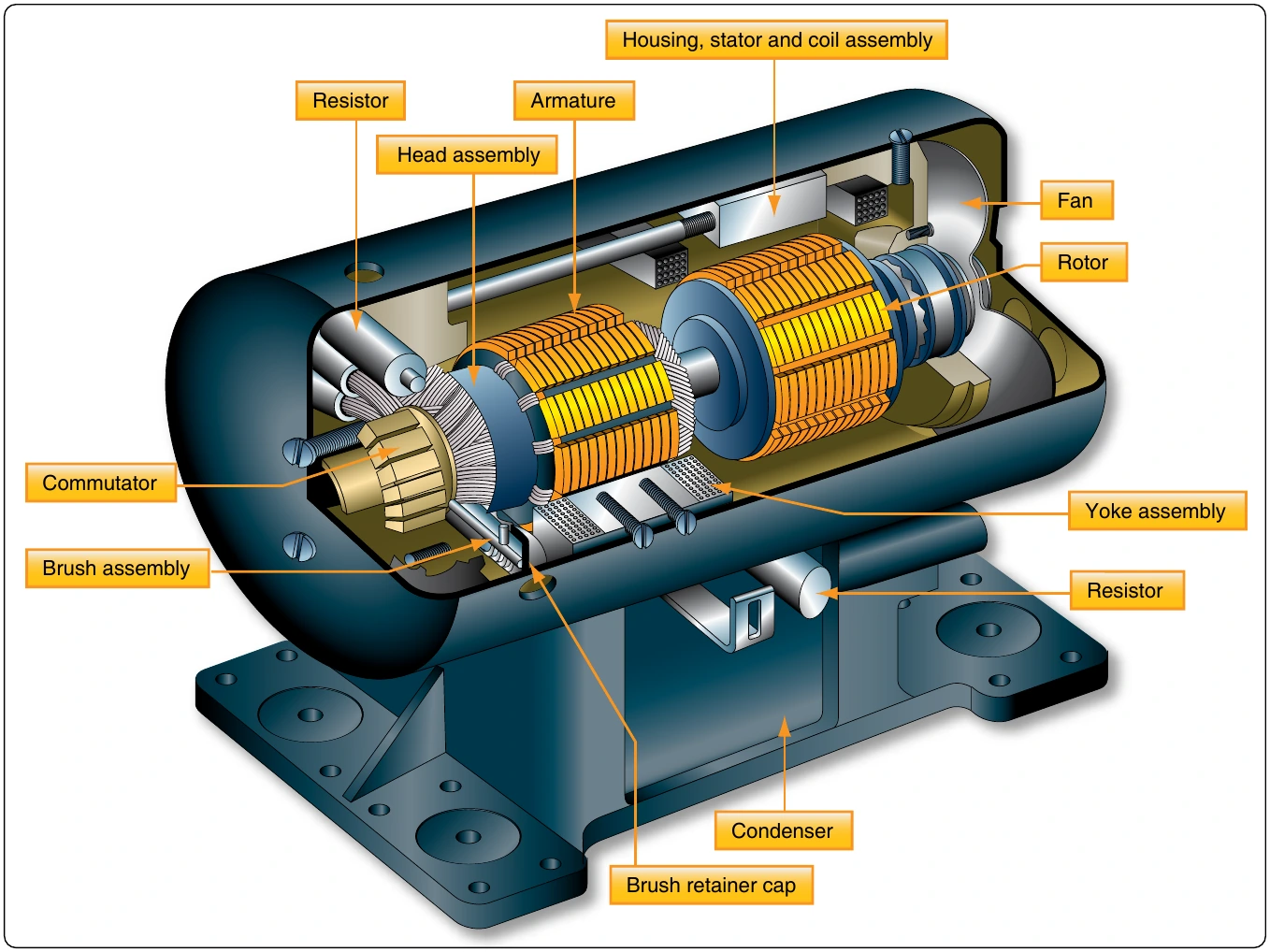
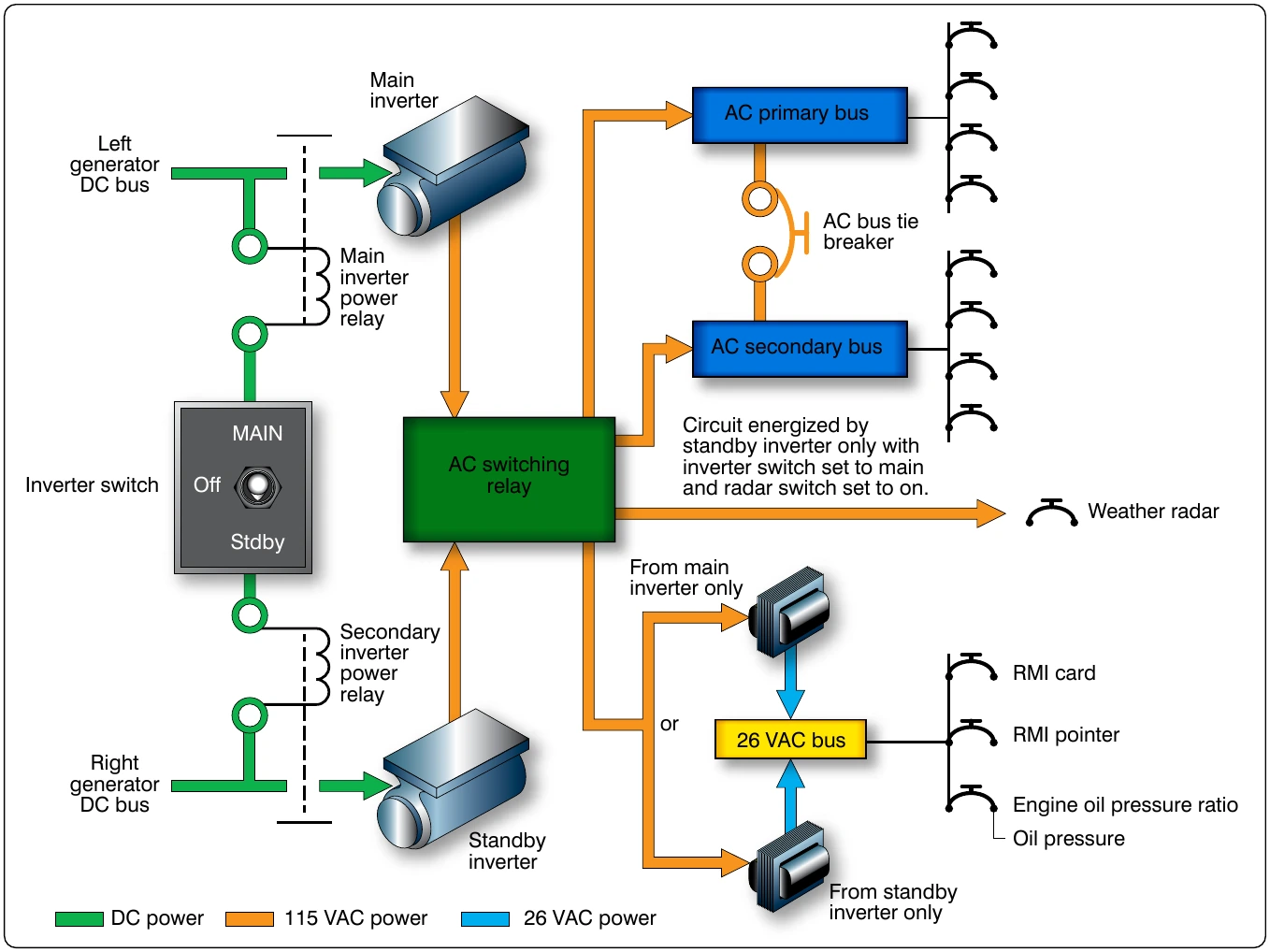
Many devices in an aircraft require high amperage, low voltage DC for operation. This power may be furnished by DC engine-driven generators, motor generator sets, vacuum main and standby rotary inverters.
tube rectifiers, or dry disk or solid-state rectifiers.
In aircraft with AC systems, a special DC generator is not desirable since it would be necessary for the engine accessory section to drive an additional piece of equipment. Motor generator sets, consisting of air-cooled AC motors that drive DC generators, eliminate this objection because they operate directly off the AC power system. Vacuum tube or various types of solid-state rectifiers provide a simple and efficient method of obtaining high voltage DC at low amperage. Dry disk and solid-state rectifiers, on the other hand, are an excellent source of high amperage at low voltage.