
Chapter 11
Communication & Navigation
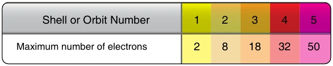
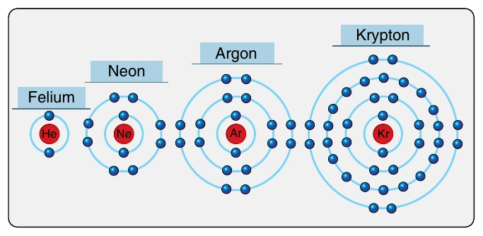
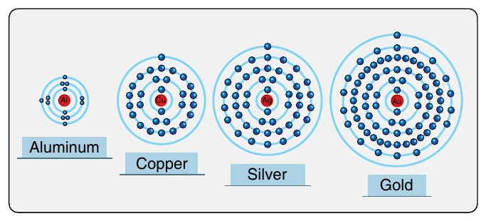
Not all materials are pure elements, that is, substances made up of one kind of atom. Compounds occur when two or more different types of atoms combine. They create a new substance with different characteristics than any of the component elements. When compounds form, valence shells and their maximum number of electrons remain the rule of physics. The new compound molecule may either share electrons to fill the valence shell or free electrons may exist to make it a good conductor.
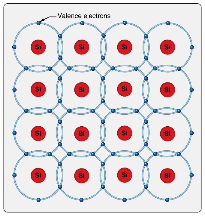
Silicon is an atomic element that contains four electrons in its valence shell. It tends to combine readily with itself and form a lattice of silicon atoms in which adjacent atoms share electrons to fill out the valance shell of each to the maximum of eight electrons. [Figure 11-16] This unique symmetric alignment of silicon atoms results in a crystalline structure.
Once bound together, the valence shells of each silicon atom are complete. In this state, movement of electrons does not occur easily. There are no free electrons to move to another atom and no space in the valence shells to accept a free electron. Therefore, silicon in this form is a good insulator.
Silicon is a primary material used in the manufacture of semiconductors. Germanium and a few other materials are also used.
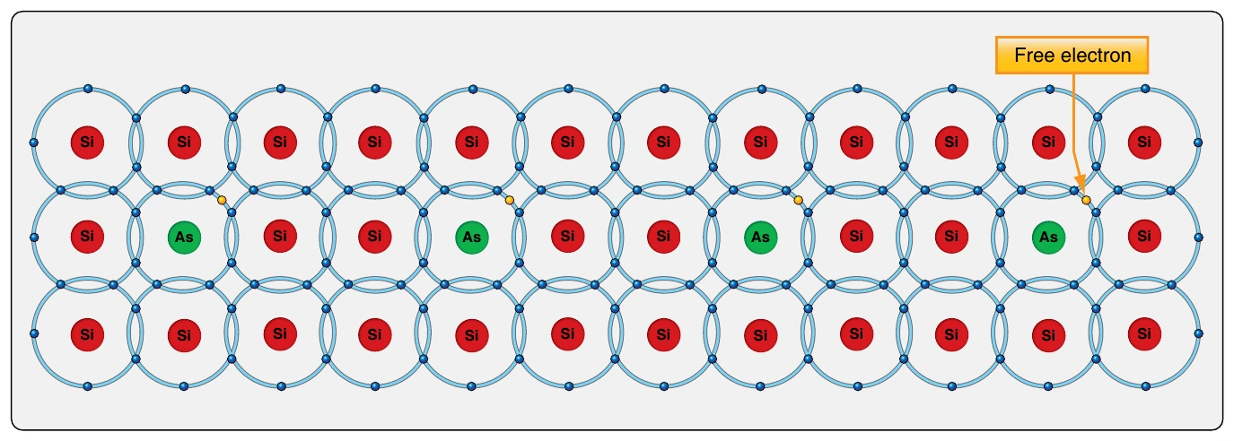
Since silicon is an insulator, it must be modified to become a semiconductor. The process often used is called doping. Starting with ultra-pure silicon crystal, arsenic, phosphorus, or some other element with five valence electrons in each atom is mixed into the silicon. The result is a silicon lattice with flaws. [Figure 11-17] The elements bond, but numerous free electrons are present in the material from the 5th electron that is part of the valence shell of the doping element atoms. These free electrons can now flow under certain conditions. Thus, the silicon becomes semiconductive. The conditions required for electron flow in a semiconductor are discussed in the following paragraphs.
When silicon is doped with an element or compound containing five electrons in its valence shell, the result is a negatively charged material due to the excess free electrons, and the fact that electrons are negatively charged. This is known as an N-type semiconductor material. It is also known as a donor material because, when it is used in electronics, it donates the extra electrons to current flow.
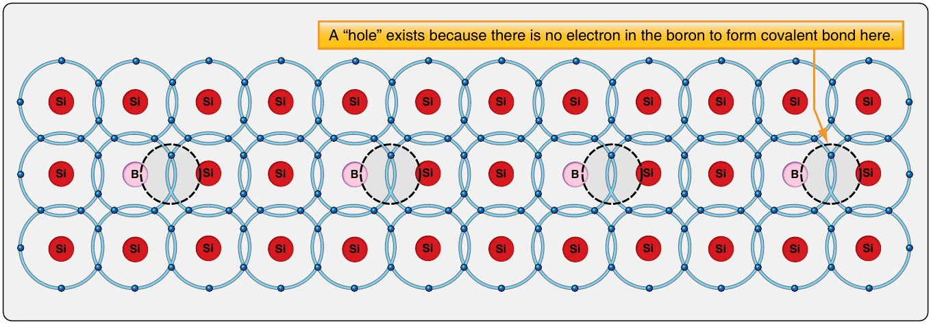
Doping silicon can also be performed with an element that has only three valence electrons, such as boron, gallium, or indium. Valence electron sharing still occurs, and the silicon atoms with interspersed doping element atoms form a lattice molecular structure. However, in this case, there are many valence shells where there are only seven electrons and not eight. This greatly changes the properties of the material. The absence of the electrons, called holes, encourages electron flow due to the preference to have eight electrons in all valence shells. Therefore, this type of doped silicon is also semiconductive. It is known as P-type material or as an acceptor since it accepts electrons in the holes under certain conditions. [Figure 11-18]
Combining N- and P-type semiconductor material in certain ways can produce very useful results. A look at various semiconductor devices follows.
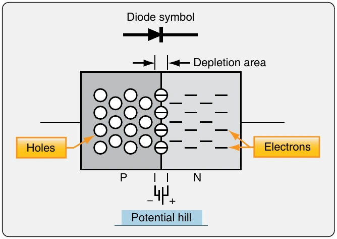
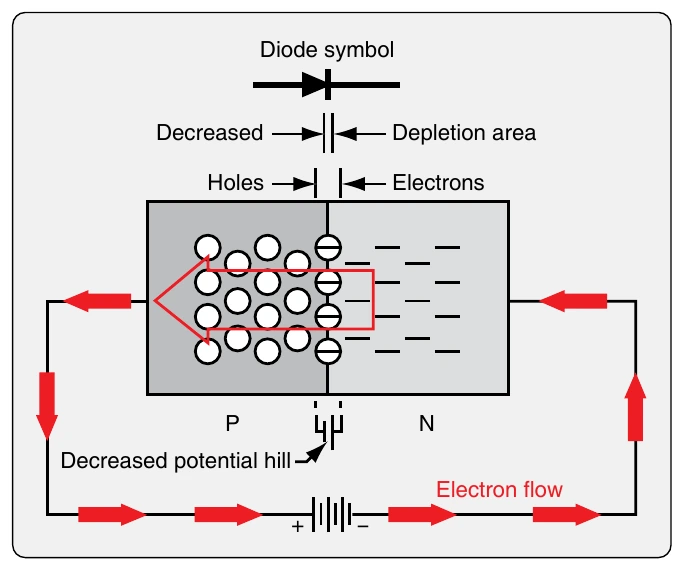
Semiconductor Diodes A diode is an electrical device that allows current to flow in one direction through the device but not the other. A simple device that can be made from N- and P-type semiconductors is a semiconductor diode. When joined, the junction of these two materials exhibits unique properties. Since there are holes in the P-type material, free electrons from the N-type material are attracted to fill these holes. Once combined, the area at the junction of the two materials where this happens is said to be depleted. There are no longer free electrons or holes. However, having given up some electrons, the N-type material next to the junction becomes slightly positively charged, and having received electrons, the P-type material next to the junction becomes slightly negatively charged. The depletion area at the junction of the two semiconductor materials constitutes a barrier or potential hill. The intensity of the potential hill is proportional to the width of the depletion area (where the electrons from the N-type material have filled holes in the P-type material). [Figure 11-19] The two semiconductors joined in this manner form a diode that can be used in an electrical circuit. A voltage source is attached to the diode. When the negative terminal of the battery is attached to the N-type semiconductor material and the positive terminal is attached to the P-type material, electricity can flow in the circuit. The negative potential of the battery forces free electrons in the N-type material toward the junction. The positive potential of the battery forces holes in the P-type material toward the other side of the junction. The holes move by the rebinding of the doping agent ions closer to the junction. At the junction, free electrons continuously arrive and fill the holes in the lattice. As this occurs, more room is available for electrons and holes to move into the area. Pushed by the potential of the battery, electrons and holes continue to combine. The depletion area becomes extremely narrow under these conditions. The potential hill or barrier is, therefore, very small. The flow of current in the electrical circuit is in the direction of electron movement shown in Figure 11-20.
In similar circuits where the negative battery terminal is attached to the N-type semiconductor material and the positive terminal is attached to the P-type material, current flows from N-type, or donor material, to P-type receptor material. This is known as a forward-biased semiconductor. A voltage of approximately 0.7 volts is needed to begin the current flow over the potential hill. Thereafter, current flow is linear with the voltage. However, temperature affects the ease at which electrons and holes combine given a specific voltage.
If the battery terminals are reversed, the semiconductor diode circuit is said to be reversed biased. [Figure 11-21] Attaching the negative terminal of the battery to the P-type material attracts the holes in the P-type material away from the junction in the diode. The positive battery terminal attached to the N-type material attracts the free electrons from the junction in the opposite direction. In this way, the width of the area of depletion at the junction of the two materials increases. The potential hill is greater. Current cannot climb the hill; therefore, no current flows in the circuit. The semiconductors do not conduct.
Semiconductor diodes are used often in electronic circuits. When AC current is applied to a semiconductor diode, current flows during one cycle of the AC but not during the other cycle. The diode, therefore, becomes a rectifier. When it is forward biased, electrons flow; when the AC cycles, electrons do not flow. A simple AC rectifier circuit containing a semiconductor diode and a load resistor is illustrated in Figure 11- 22. Semiconductor diode symbols and examples of semiconductor diodes are shown in Figure 11-23.