Chapter 11
Communication & Navigation
Combination of semiconductor materials is not limited to a two-type, three-layer sandwich transistor. By creating a four-layer sandwich of alternating types of semiconductor material (i.e., PNPN or NPNP), a slightly different semiconductor diode is created. As is the case in a two-layer diode, circuit current is either blocked or permitted to flow through the diode in a single direction.
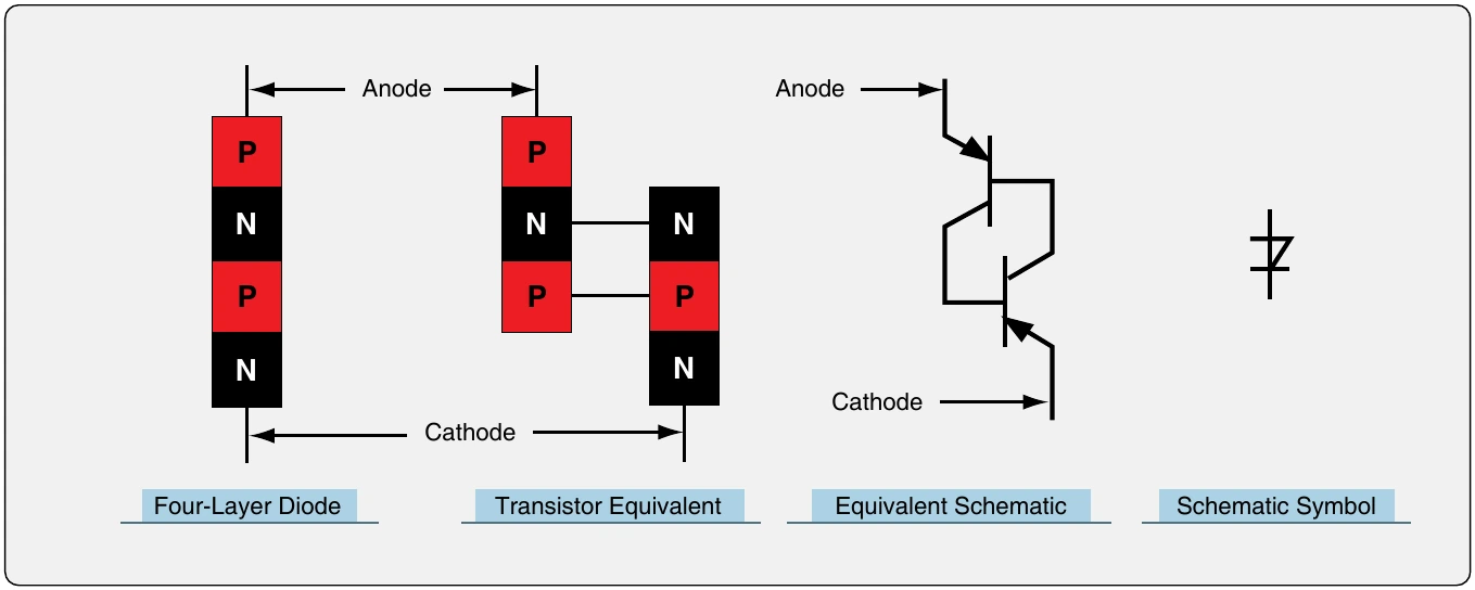
Within a four-layer diode, sometimes known as a Shockley diode, there are three junctions. The behavior of the junctions and the entire four-layer diode can be understood by considering it to be two interconnected three-layer transistors. [Figure 11-28] Transistor behavior includes no current flow until the base material receives an applied voltage to narrow the depletion area at the base-emitter junction. The base materials in the four-layer diode transistor model receive charge from the other transistor’s collector. With no other means of reducing any of the depletion areas at the junctions, it appears that current does not flow in either direction in this device. However, if a large voltage is applied to forward bias the anode or cathode, at some point the ability to block flow breaks down. Current flows through whichever transistor is charged. Collector current then charges the base of the other transistor and current flows through the entire device.
Some caveats are necessary with this explanation. The transistors that comprise this four-layer diode must be constructed of material similar to that described in a zener diode. That is, it must be able to endure the current flow without burning out. In this case, the voltage that causes the diode to conduct is known as breakover voltage rather than breakdown voltage. Additionally, this diode has the unique characteristic of allowing current flow to continue until the applied voltage is reduced significantly, in most cases, until it is reduced to zero. In AC circuits, this would occur when the AC cycles.
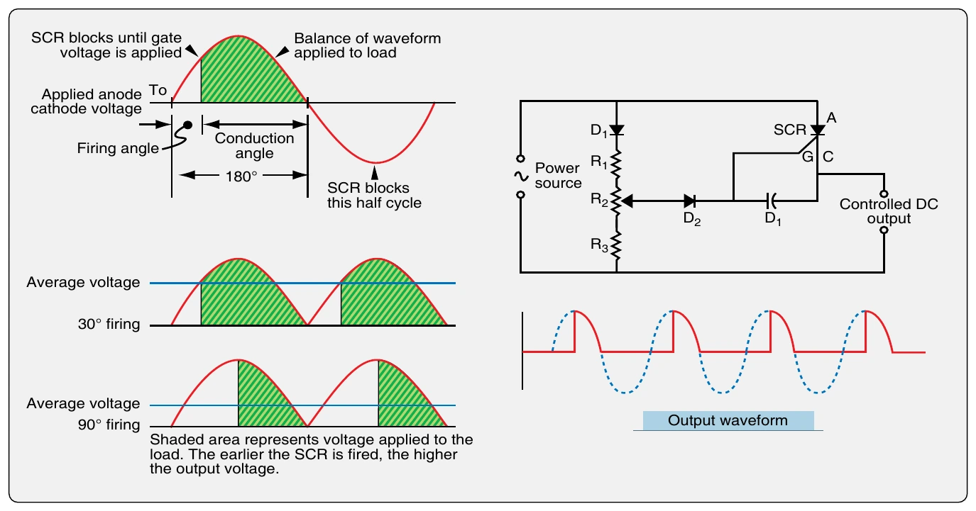
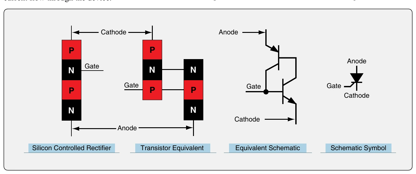
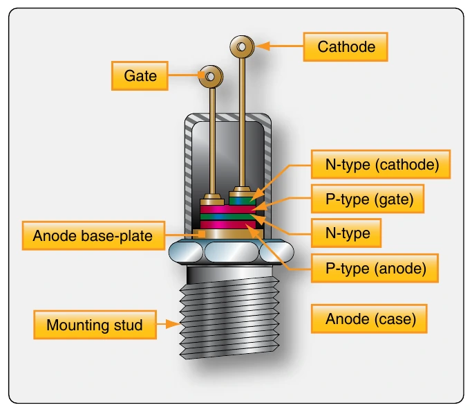
While the four-layer, Shockley diode is useful as a switching device, a slight modification to its design creates a silicon-controlled rectifier (SCR). To construct a SCR, an additional terminal known as a gate is added. It provides more control and utility. In the four-layer semiconductor construction, there are always two junctions forward biased and one junction reversed biased. The added terminal allows the momentary application of voltage to the reversed biased junction. All three junctions then become forward biased and current at the anode flows through the device. Once voltage is applied to the gate, the SCR become latched or locked on. Current continues to flow through it until the level drops off significantly, usually to zero. Then, another applied voltage through the gate is needed to reactivate the current flow. [Figures 11-29 and 11-30]
SCRs are often used in high voltage situations, such as power switching, phase controls, battery chargers, and inverter circuits. They can be used to produce variable DC voltages for motors and are found in welding power supplies. Often, lighting dimmer systems use SCRs to reduce the average voltage applied to the lights by only allowing current flow during part of the AC cycle. This is controlled by controlling the pulses to the SCR gate and eliminating the massive heat dissipation caused when using resistors to reduce voltage. Figure 11-31 graphically depicts the timing of the gate pulse that limits full cycle voltage to the load. By controlling the phase during which, time the SCR is latched, a reduced average voltage is applied.
Triacs
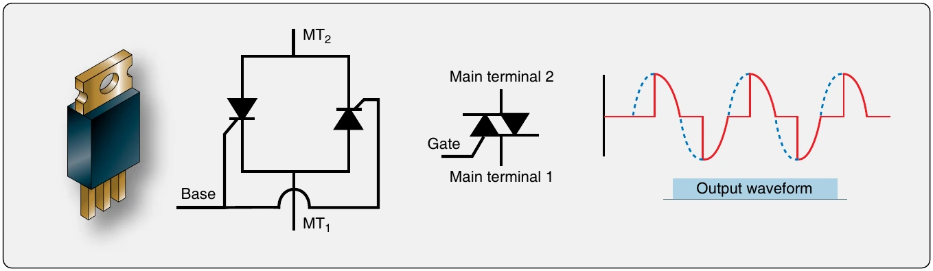
SCRs are limited to allowing current flow in one direction only. In AC circuitry, this means only half of the voltage cycle can be used and controlled. To access the voltage in the reverse cycle from an AC power source, a triac can be used. A triac is also a four-layer semiconductor device. It differs from an SCR in that it allows current flow in both directions. A triac has a gate that works the same way as in a SCR; however, a positive or negative pulse to the gate triggers current flow in a triac. The pulse polarity determines the direction of the Figure 11-32 illustrates a triac and shows a triac in a simple circuit. It can be triggered with a pulse of either polarity and remains latched until the voltage declines, such as when the AC cycles. Then, it needs to be triggered again. In many ways, the triac acts as though it is two SCRs connected side by side only in opposite directions. Like an SCR, the timing of gate pulses determines the amount of the total voltage that is allowed to pass. The output waveform if triggered at 90° is shown in Figure 11-32. Because a triac allows current to flow in both directions, the reverse cycle of AC voltage can also be used and controlled.
When used in actual circuits, triacs do not always maintain the same phase firing point in reverse as they do when fired with a positive pulse. This problem can be regulated somewhat through the use of a capacitor and a diac in the required, two SCRs in reverse of each other are often used instead of the triac. Triacs do perform well in lower voltage circuits. Figure 11-33 illustrates the semiconductor layering in a triac.
Unijunction Transistors (UJT)
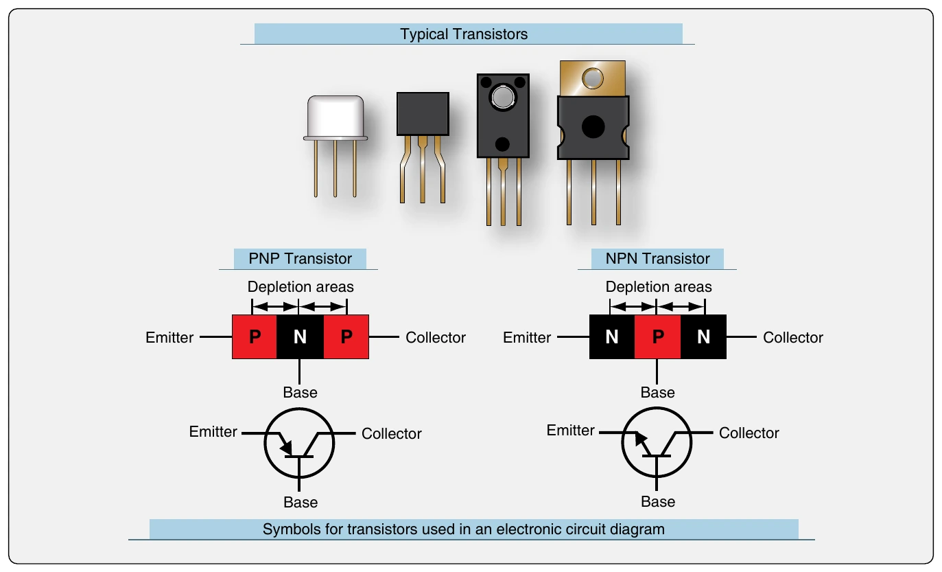
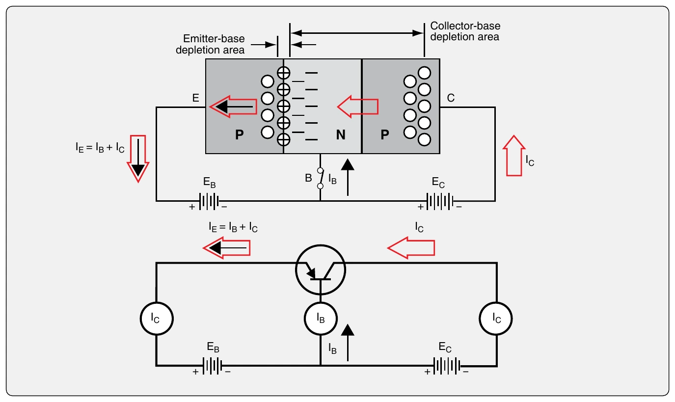
The behavior of semiconductor materials is exploited through the construction of numerous transistor devices containing various configurations of N-type and P-type materials. The physical arrangement of the materials in relation to each other yields devices with unique behaviors and applications. The transistors described above having two junctions of P-type and N-type materials (PN) are known as bipolar junction transistors. Other more simple transistors can be fashioned with only one junction of the PN semiconductor materials. These are known as unijunction transistors (UJT). [Figure 11-34]
The UJT contains one base semiconductor material and a different type of emitter semiconductor material. There is no collector material. One electrode is attached to the emitter and two electrodes are attached to the base material at opposite ends. These are known as base 1 (B1) and base 2 (B2). The electrode configuration makes the UJT appear physically the same as a bipolar junction transistor. However, there is only one PN junction in the UJT and it behaves differently.
The base material of a UJT behaves like a resistor between the electrodes. With B2 positive with respect to B1, voltage gradually drops as it flows through the base. [Figure 11-35] By placing the emitter at a precise location along the base material gradient, the amount of voltage needed to be applied to the emitter electrode to forward bias the UJT base-emitter junction is determined. When the applied emitter voltage exceeds the voltage at the gradient point where the emitter is attached, the junction is forward biased and current flows freely from the B1 electrode to the E electrode. Otherwise, the junction is reversed biased and no significant current flows although there is some leakage. By selecting a UJT with the correct bias level for a particular circuit, the applied emitter voltage can control current flow through the device.