
Chapter 11
Communication & Navigation
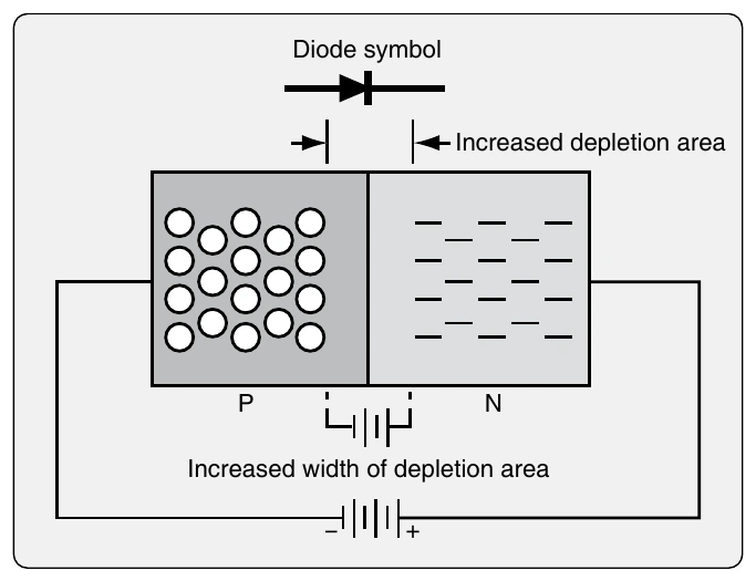
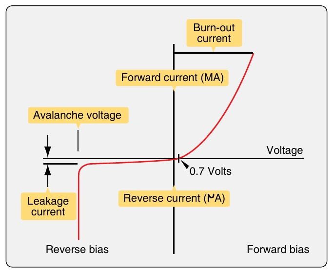
Semiconductor diodes have limitations. They are rated for a range of current flow. Above a certain level, the diode overheats and burns up. The amount of current that passes through the diode when forward biased is directly proportional to the amount of voltage applied. But, as mentioned, it is affected by temperature.
Figure 11-24 indicates the actual behavior of a semiconductor diode. In practice, a small amount of current does flow through a semiconductor diode when reversed biased. This is known as leakage current and it is in the micro amperage range. However, at a certain voltage, the blockage of current flow in a reversed biased diode breaks down completely. This voltage is known as the avalanche voltage because the diode can no longer hold back the current and the diode fails.
Zener Diodes
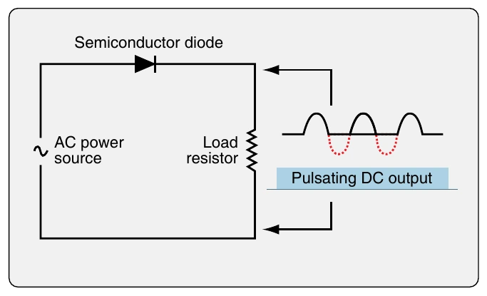
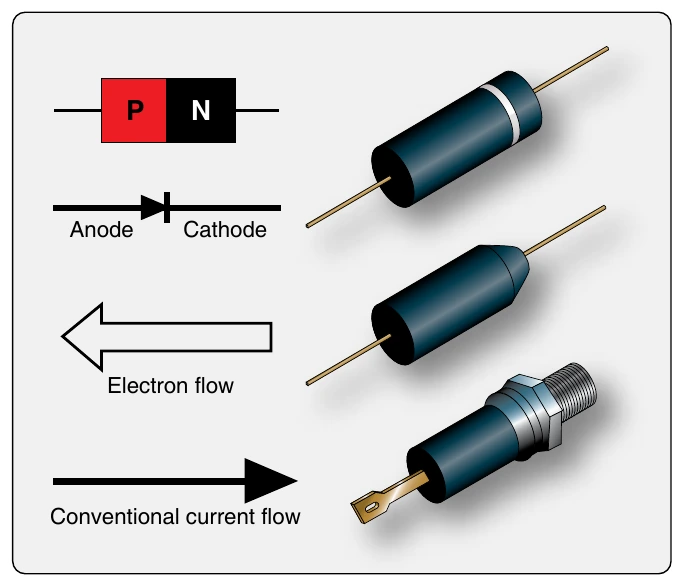
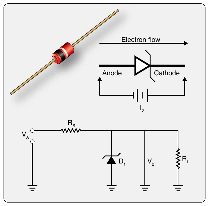
Diodes can be designed with a zener voltage. This is similar to avalanche flow. When reversed biased, only leakage current flows through the diode. However, as the voltage is increased, the zener voltage is reached. The diode lets current flow freely through the diode in the direction in which it is normally blocked. The diode is constructed to be able to handle the zener voltage and the resulting current, whereas avalanche voltage burns out a diode. A zener diode can be used as means of dropping voltage or voltage regulation. It can be used to step down circuit voltage for a particular application but only when certain input conditions exist. Zener diodes are constructed to handle a wide range of voltages. [Figure 11-25]
Transistors
While diodes are very useful in electronic circuits, semiconductors can be used to construct true control valves known as transistors. A transistor is little more than a sandwich of N-type semiconductor material between two pieces of P-type semiconductor material or vice versa. However, a transistor exhibits some remarkable properties and is the building block of all things electronic. [Figure 11-26] As with any union of dissimilar types of semiconductor materials, the junctions of the P- and N- materials in a transistor have depletion areas that create potential hills for the flow of electrical charges.
Like a vacuum tube triode, the transistor has three electrodes or terminals, one each for the three layers of semiconductor material. The emitter and the collector are on the outside of the sandwiched semiconductor material. The center material is known as the base. A change in a relatively small amount of voltage applied to the base of the transistor allows a relatively large amount of current to flow from the collector to the emitter. In this way, the transistor acts as a switch with a small input voltage controlling a large amount of current.
If a transistor is put into a simple battery circuit, such as the one shown in Figure 11-27, voltage from the battery (EB) forces free electrons and holes toward the junction between the base and the emitter just as it does in the junction of a semiconductor diode. The emitter-base depletion area becomes narrow as free electrons combine with the holes at the junction. Current (IB) (solid arrows) flows through the junction in the emitter-base battery circuit. At the same time, an emitter-collector circuit is constructed with a battery (EC) of much higher voltage in its circuit. Because of the narrow depletion area at the emitter-base junction, current IC is able to cross the collector base junction, flow through emitter-base junction, and complete the collector-emitter battery circuit (hollow arrows).
To some extent, varying the voltage to the base material can increase or decrease the current flow through the transistor as the emitter-base depletion area changes width in response to the base voltage. If base voltage is removed, the emitter-base depletion area becomes too wide and all current flow through the transistor ceases.
Current in the transistor circuit illustrated has a relationship
the voltage applied to the base that turns the collector-emitter transistor current on or off.
Controlling a large amount of current flow with a small independent input voltage is very useful when building electronic circuits. Transistors are the building blocks from which all electronic devices are made, including Boolean gates that are used to create microprocessor chips. As production techniques have developed, the size of reliable transistors has shrunk. Now, hundreds of millions and even billions of transistors may be used to construct a single chip such as the one that powers your computer and various avionic devices.