
Chapter 11
Communication & Navigation
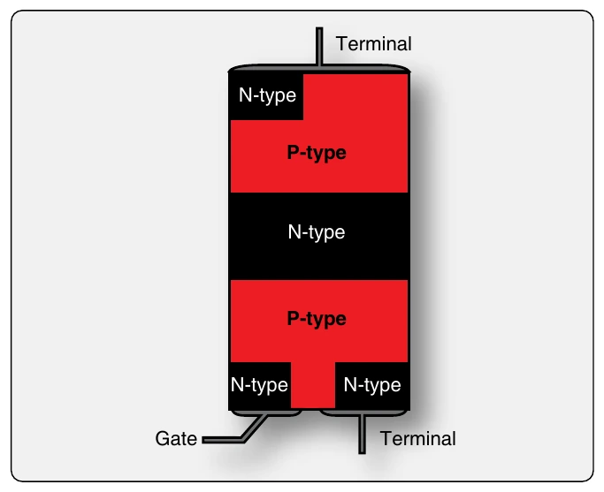
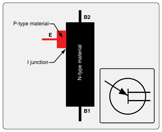
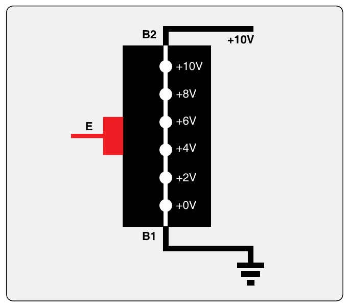
UJTs of a wide variety of designs and characteristics exist. A description of all of them is beyond the scope of this discussion. In general, UJTs have some advantages over bipolar transistors. They are stable in a wide range of temperatures. In some circuits, use of UJTs can reduce the overall number of components used, which saves money and potentially increases reliability. They can be found in switching circuits, oscillators, and wave shaping circuits. However, four-layered semiconductor thyristors that function the same as the UJT just described are less expensive and most often used.
Field Effect Transistors (FET)
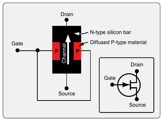
As shown in the triac and the UJT, creative arrangement of semiconductor material types can yield devices with a variety of characteristics. The field effect transistor (FET) is another such device which is commonly used in electronic circuits. Its N- and P-type material configuration is shown in Figure 11-36. A FET contains only one junction of the two types of semiconductor material. It is located at the gate where it contacts the main current carrying portion of the device. Because of this, when an FET has a PN junction, it is known as a junction field effect transistor (JFET). All FETs operate by expanding and contracting the depletion area at the junction of the semiconductor materials.
One of the materials in a FET or JFET is called the channel. It is usually the substrate through which the current needing to be controlled flows from a source terminal to a drain terminal. The other type of material intrudes into the channel and acts as the gate. The polarity and amount of voltage applied to the gate can widen or narrow the channel due to expansion or shrinking of the depletion area at the junction of the semiconductors. This increases or decreases the amount of current that can flow through the channel. Enough reversed biased voltage can be applied to the gate to prevent the flow of current through the channel. This allows the FET to act as a switch. It can also be used as a voltage-controlled resistance.
FETs are easier to manufacture than bipolar transistors and have the advantage of staying on once current flow begins without continuous gate voltage applied. They have higher impedance than bipolar transistors and operate cooler. This makes their use ideal for integrated circuits where millions of FETs may be in use on the same chip. FETs come in N-channel and P-channel varieties.
Metal Oxide Semiconductor Field Effect Transistors (MOSFETs) & Complementary Metal Oxide Semiconductor (CMOS)
The basic FET has been modified in numerous ways and continues to be at the center of faster and smaller electronic component development. A version of the FET widely used is the metal oxide semiconductor field effect transistor (MOSFET). The MOSFET uses a metal gate with a thin insulating material between the gate and the semiconductor material. This essentially creates a capacitor at the gate and eliminates current leakage in this area. Modern versions of the MOSFET have a silicon dioxide insulating layer and many have poly-crystalline silicon gates rather than metal, but the MOSFET name remains and the basic behavioral characteristic are the same. [Figure 11-37]
As with FETs, MOSFETs come with N-channels or P-channels. They can also be constructed as depletion mode or enhancement mode devices. This is analogous to a switch being normally open or normally closed. Depletion mode MOSFETs have an open channel that is restricted or closed when voltage is applied to the gate (i.e., normally open). Enhancement mode MOSFETs allow no current to flow at zero bias but create a channel for current flow when voltage is applied to the gate (normally closed). No voltage is used when the MOSFETs are at zero bias. Millions of enhancement mode MOSFETs are used in the construction of integrated circuits. They are installed in complimentary pairs such that when one is open, the other is closed. This basic design is known as complementary MOSFET (CMOS), which is the basis for integrated circuit design in nearly all modern electronics. Through the use of these transistors, digital logic gates can be formed, and digital circuitry is constructed.
Other more specialized FETs exist. Some of their unique characteristics are owed to design alterations and others to material variations. The transistor devices discussed above use silicon-based semiconductors. But the use of other semiconductor materials can yield variations in performance. Metal semiconductor FETs (MESFETS) for example, are often used in microwave applications. They have a combined metal and semiconductor material at the gate and are typically made from gallium arsenide or indium phosphide. MESFETs are used for their quickness when starting and stopping current flows especially in opposite directions. High electron mobility transistors (HEMT) and pseudomorphic high electron mobility transistors (PHEMT) are also constructed from gallium arsenide semiconductor material and are used for high-frequency applications.
Photodiodes & Phototransistors
Light contains electromagnetic energy that is carried by photons. The amount of energy depends on the frequency of light of the photon. This energy can be very useful in the operation of electronic devices since all semiconductors are affected by light energy. When a photon strikes a semiconductor atom, it raises the energy level above what is needed to hold its electrons in orbit. The extra energy frees an electron enabling it to flow as current. The vacated position of the electron becomes a hole. In photodiodes, this occurs in the depletion area of the reversed biased PN junction turning on the device and allowing current to flow.
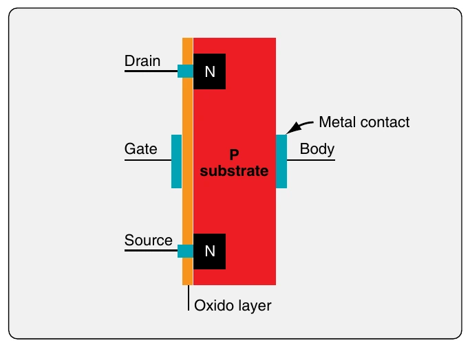
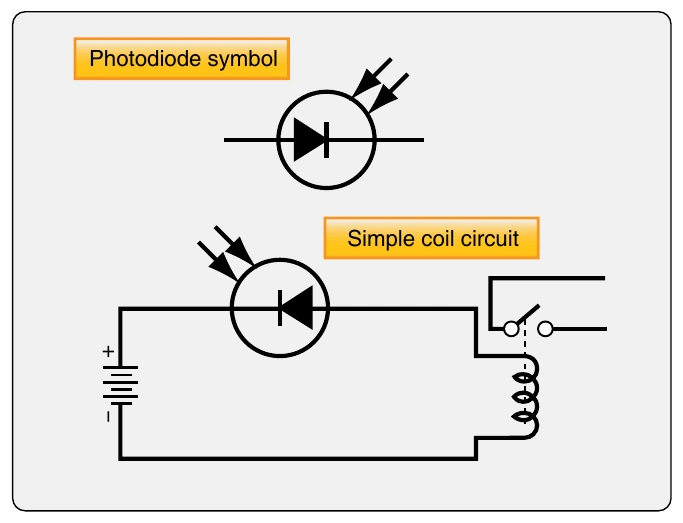
Figure 11-38 illustrates a photodiode in a coil circuit. In this case, the light striking the photodiode causes current to flow in the circuit whereas the diode would have otherwise blocked it. The result is the coil energizes and closes another circuit enabling its operation.
A photon activated transistor could be used to carry even more current than a photodiode. In this case, the light energy is focused on a collector-base junction. This frees electrons in the depletion area and starts a flow of electrons from the base that turns on the transistor. Once on, heavier current flows from the emitter to the collector. [Figure 11-39] In practice, engineers have developed numerous ways to use the energy in light photons to trigger semiconductor devices in electronic circuits. [Figure 11-40]